


Quick-Turn, Standard & Advanced PCBs A Comprehensive Comparative Guide
In the world of electronics, printed circuit boards (PCBs) function like the human nervous system—carrying signals and power throughout devices. But did you know that behind every seemingly ordinary circuit board lies distinct manufacturing worlds, ranging from lightning-fast delivery to precision engineering? When engineers navigate different product development stages, three primary PCB types—Quick-Turn PCBs, Standard PCBs, and Advanced PCBs—serve as specialized tools, each striking a unique balance between speed, cost, and performance.
Quick Turn PCB: Core Definitions & Applications & Fundamental Differences
1.Quick-Turn PCBs: The Speed Pioneers
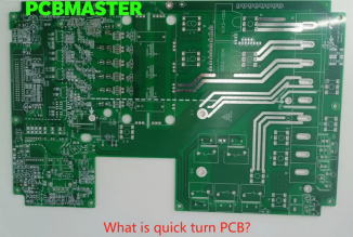
Built for time-critical R&D phases, these boards deliver prototypes in 24 hours to 5 days. Typically ≤8 layers with standard FR-4 substrates, they avoid complex features like blind/buried vias. Their mission: rapid functional validation—akin to architectural mock-ups prioritizing speed over refinement.
Example scenario: A startup developing a smart home controller needs 10 demo boards for an exhibition. Quick-turn manufacturing delivers boards from Gerber files within 48 hours. To get started with your own quick-turn PCB order, simply request a quote online—getting your prototype is fast and straightforward with instant pricing and step-by-step guidance.
2.Standard PCBs: The Economical Workhorses
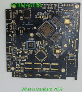
When products enter mass production, standard PCBs become the cost-optimized solution. Using common 1-12 layer FR-4 materials with HASL or OSP finishes, they comply with IPC Class 2 standards. Lead times and costs are based on design complexity or order size, typically spanning 1-4 weeks, though bulk orders significantly reduce per-unit costs.
The charging brick for your phone or your office wireless keyboard likely contains a standard PCB—balancing reliability and cost efficiency.
3.Advanced PCBs: The Technological Vanguard
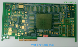
For applications like 5G base stations, autonomous vehicles, or aerospace systems, advanced PCBs excel. These utilize specialized materials (Rogers, Taconic), metal cores (Al/Cu), or flex substrates, supporting HDI routing, blind/buried vias, and 3D packaging. Compliance with IPC Class 3, IATF 16949, or ISO 13485 standards is mandatory. Lead times exceed 4 weeks, with costs often multiples of standard boards.
Consider: The control board inside a medical CT scanner—requiring flawless signal integrity under high radiation—exemplifies advanced PCB applications.
PCB Manufacturing Process: From Blueprint to Board
The journey of a printed circuit board from concept to finished product is a multi-stage process that demands precision, advanced technology, and strict quality control. It all begins with the design phase, where engineers use specialized software to lay out the circuitry, define the number of layers, select the right materials—such as FR-4 for standard boards or advanced substrates for high-performance applications—and determine the placement of vias and holes. This blueprint forms the foundation for the entire pcb manufacturing process.
Once the design is finalized, a photoplot is generated to transfer the circuit pattern onto the board. The raw board material is then cut and drilled to exact specifications, creating the necessary holes for component leads and vias. Next, a layer of copper is applied using electroplating, ensuring high conductivity and robust connections across all layers. The copper is then precisely etched to form the intricate circuit paths that define the board’s functionality.
To protect the circuits and enhance durability, a protective plating—such as HASL, OSP, or ENIG—is added. The board then moves to the assembly stage, where components are mounted using either surface mount technology (SMT) for high-density designs or through-hole technology (THT) for added mechanical strength. For advanced pcb requirements, such as rigid flex or high-density interconnect (HDI) boards, specialized equipment and processes are used to achieve the highest quality and reliability, supporting complex, multi-layer circuits and demanding applications.
Throughout every step, rigorous testing and inspection ensure that each circuit board meets industry standards for quality and performance. Whether producing a simple two-layer prototype or a multi-layer advanced pcb for aerospace or medical use, the manufacturing process is engineered for precision, efficiency, and high reliability—delivering boards that power the world’s most innovative electronics.
Production Timelines: The Time-Cost Tradeoff
Production Phase | Quick-Turn PCBs | Standard PCBs | Advanced PCBs |
Prototyping Lead Time | 24hrs–5 days | 5–7 days | 7–15 days |
Mass Production | N/A | 2–4 weeks (1k+ units) | 4–8 weeks (special processes) |
Rush Service | 12hr ultra-rush (+30–50% fee) | Limited (+20–40% fee) | Generally unavailable |
Key Characteristics | • Skipped DFM review\ • Express scheduling\ • Generic parameters | • Full process prep\ • Batch scheduling\ • Standard QC | • Multi-stage engineering\ • Exotic material sourcing\ • Segmented process con |
Behind quick-turn speed: Streamlined processes—minimal DFM checks, stocked materials, and reduced testing. Turnaround times are based on the specific requirements of your project or the complexity of the design. Like fast-food kitchens: efficient but inflexible. Engineer’s quip: “Submitted Gerbers at night; received shipping notification before my morning coffee!”
Advanced PCB delays stem from: Precision processes—e.g., a 20-layer server board may require >30 steps: laser drilling → pulse plating → sequential lamination → X-ray alignment. Each demands parameter perfection—comparable to Swiss watchmaking.
Quality Standards: From Functional to Fail-Safe
1. Quick-Turn: "Fit-for-Purpose" Philosophy
Testing: Sampled flying probe + AOI.
Tolerances:
·Line width: ±20%
·Impedance: ±10Ω
Reality check: A drone maker learned the hard way—quick-turn prototypes passed functional tests but failed in high-altitude temperature swings, causing batch recalls.
2. Standard: The Balanced Approach
Compliance: IPC Class 2
Testing: 100% flying probe + full AOI
Tolerances:
·Line width: ±15%
·Hole position: ±0.05mm
Limitation: Standard FR-4 may delaminate in extreme cold (–40°C).
3. Advanced: "Zero-Failure" Mandate
Testing resembles scientific experimentation:
·Signal integrity: 100Gbps eye diagrams
·Reliability: 1,000x thermal cycles (–55°C↔125°C)
·Microscopy: 3D X-ray solder void analysis
·Destructive tests: Peel strength, CAF resistance
Case: A military PCB requiring 20-year MRI-environment operation underwent 127 tests, including 45-day environmental trials.
Cost Structures: Decoding the Price Matrix

1. Quick-Turn: Fixed-Cost Dominated
·Engineering fees ≈30% ($43–$86 even for 1 board)
·Rush premiums: 20–50% (nightshift premiums)
·Low material utilization (≤40% for irregular shapes)
Example: 10pcs 10x10cm 2-layer board
✓ Standard lead: $40
✓24hr rush: $60 (+50%)
2. Standard: Economies of Scale
·Materials = 60–70% (price fluctuates with FR-4)
·Tooling amortization: Test fixtures ($145), stamping molds ($215)
·Volume discounts: 1k-unit price ≈40% below 100-unit
Optimization tips:
✓ Panelization → 85% material utilization
✓ Avoid micro-vias <0.2mm
✓ Choose HASL over ENIG
3. Advanced: Technology Premium
·Exotic materials: Rogers substrates cost 8–12× FR-4
·Precision equipment: Laser drills >$58/hour
Cost drivers:
✓ Any-layer HDI (+$30/m²)
✓ Copper ≥3oz (+30%/oz)
✓ 100% impedance test (+$0.035/point)
Cost Type | Quick-Turn (5pcs) | Standard (1kpcs) | Advanced (100pcs) |
Unit Price | $26 | $6 | $90 |
Engineering % | 32% | 1.5% | 8% |
Materials % | 28% | 68% | 55% |
Special Processes | – | – | 25% |
Testing % | 5% | 7% | 12% |
Table: Cost Breakdown (10x10cm 4-layer basis)
Selection Strategy: Matching Needs to Solutions
1. When to Choose Quick-Turn
·Prototyping: Functional verification in ≤3 days
·Design iterations: >5 revisions expected
·Emergency replacement: Production line shortages
Design constraints:
→ Avoid >2A power traces (copper thickness limits)
→ Use for RF basic functionality only
2. Standard PCB Sweet Spots
·Consumer electronics mass production
·Cost-sensitive projects (<35% margin)
·Stable environments (indoor/consumer)
Design hacks:
✓ Size boards as 100x100mm multiples (reduced milling fees)
✓ Standardize hole sizes (minimize drill changes)
3. Advanced PCB Necessities
·Extreme environments: Automotive engine bays (–40°C–150°C)
·Life-critical devices: Pacemakers
·High-frequency systems: 77GHz radar
Success factors:
✓ Collaborate with fabricators 8+ weeks pre-production
✓ Budget 10% cost contingency
✓ Phased certifications (Class 3 → military specs)
Technical Specification Comparison
Parameter | Quick-Turn PCBs | Standard PCBs | Advanced PCBs |
Typical Use | Functional prototypes | Consumer electronics | 5G/Medical/Aerospace |
Lead Time | ★★★★★ (24h–5d) | ★★★☆☆ (1–4w) | ★★☆☆☆ (4–8w) |
Cost Efficiency | ★★☆☆☆ (High per-unit) | ★★★★★ (Bulk-optimized) | ★★☆☆☆ (Significant premium) |
Quality Std | ★★☆☆☆ (IPC Class 1) | ★★★☆☆ (IPC Class 2) | ★★★★★ (IPC Class 3+) |
Complexity | ★☆☆☆☆ (≤8L, no BVHs) | ★★★☆☆ (≤12L, PTH) | ★★★★★ (Any-layer HDI) |
Materials | Stock FR-4 | FR-4 (customizable) | HF/Metal-core/Ceramic |
Design Freedom | Restricted (≥4mil) | Moderate (≥3.5mil) | High (≤2.4mil) |
Reliability | Short-term indoor | 5–8 years | 15+ years / extreme env. |
Environmental Considerations: Sustainability in PCB Choices
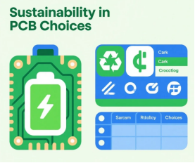
As the electronics industry evolves, sustainability has become a key factor in printed circuit board design and manufacturing. The production of circuit boards traditionally involves materials and processes that can impact the environment, including the use of hazardous substances like lead and the generation of manufacturing waste. Today, leading pcb manufacturing companies are adopting greener practices to minimize their environmental footprint while maintaining high quality and reliability.
One major shift is the move toward lead-free materials and the adoption of environmentally friendly laminates such as FR-4, which combines glass fiber and epoxy resin for durability and recyclability. Advanced pcb manufacturers are also optimizing their processes to reduce waste, implementing recycling programs, and designing boards with end-of-life recovery in mind. By selecting materials that are easier to recycle and reusing production scrap, companies can significantly cut down on landfill contributions.
Energy efficiency is another focus area. Modern pcb manufacturing facilities invest in state-of-the-art equipment that uses less power and generates fewer emissions, supporting both quick turn and high-volume production with a reduced carbon footprint. Lean manufacturing techniques further streamline production, minimizing resource use and maximizing output quality.
For businesses seeking high reliability and performance in their products, choosing a manufacturer that prioritizes sustainability offers dual benefits: environmental responsibility and advanced technical support. Quick turn and advanced pcb services can guide customers in selecting eco-friendly materials, optimizing board design for recyclability, and ensuring compliance with global environmental standards. By making sustainability a core part of the pcb manufacturing process, companies not only protect the planet but also enhance the long-term quality and reliability of their products—meeting the needs of today’s market and tomorrow’s world.
Conclusion: Mastering the Speed-Cost-Performance Triangle
As electronics innovation accelerates, PCB selection has become a critical strategic decision. Quick-turn PCBs are sprinters—capturing market opportunities through speed. Standard PCBs are marathon runners—enabling scalable production. Advanced PCBs mountaineers—conquering technological extremes.
Savvy engineers embrace phased strategies:
·Use quick-turn boards for smartwatch algorithm validation (5 iterations)
·Switch to standard PCBs for mass production (40% cost reduction via panelization)
·Deploy advanced PCBs in implantable glucose sensors—where 5× cost justifies medical certification
This tiered approach epitomizes electronics innovation wisdom: finding your product’s optimal balance within the impossible triangle of speed, cost, and performance. Next time you design a board, ask: Which PCB type truly serves this development phase? The answer lies in mastering these three distinct solutions.
FQAs
Q:What is Quick-Turn PCB?
A:Quick-Turn Printed Circuit Boards (PCBs) are circuit boards designed, manufactured, assembled, and tested within a very short timeframe. Their main advantage lies in enabling rapid response to project demands, making them ideal for prototyping during design iterations and significantly accelerating product development.
Q:What is the lead time for Quick-Turn PCBs?
A:Lead times typically range from 24 to 72 hours, depending on the design complexity and the quantity of boards required. While more complex designs or larger quantities may extend the timeline slightly, the service is fundamentally designed to meet the needs of time-sensitive projects.
Q:How does the cost of Quick-Turn PCB compare to standard production?
A:Due to the expedited nature of the service, Quick-Turn PCBs generally cost more than standard production. This premium reflects the need to allocate dedicated resources and prioritize manufacturing slots. However, the value of rapid delivery is critical for businesses needing parts urgently.
Q:How is quality ensured for Quick-Turn PCBs?
A:Quality is maintained through strict control measures, including Automated Optical Inspection (AOI) and electrical testing. AOI detects visual defects, while electrical testing verifies circuit functionality. Rigorous quality checks are implemented at every stage, from raw materials to finished boards, ensuring high-quality delivery even under tight deadlines.
Q:When is standard PCB service appropriate?
A:Standard PCB service is best suited once a product moves from the prototype phase into volume production. At this stage, the design is finalized, and standard PCB manufacturing offers a more cost-effective solution for larger quantities while maintaining product consistency and quality.
Q:What about manufacturing tolerances for standard PCBs?
A:Standard PCB services typically adhere to tighter manufacturing tolerances. This means stricter control over dimensional accuracy, trace alignment, and other critical parameters during fabrication. This enhanced precision improves product reliability and stability, ensuring consistent quality across high-volume production runs.
Q:What are the advantages of choosing standard PCB?
A:After prototypes are tested and the final design is confirmed, standard PCBs offer significant advantages for bulk orders. They enable cost-effective mass production, undergo rigorous internal quality assurance testing to meet industry standards, ensure product reliability and performance, and leverage economies of scale to reduce overall unit costs.
Q:What is the main difference between Advanced PCBs and standard PCBs?
A:Advanced PCBs utilize more sophisticated manufacturing processes and offer superior performance and functionality. They often incorporate precision techniques like higher-resolution imaging, complex multi-layer interconnects (HDI), and advanced materials. This allows them to meet demanding requirements for high-speed signal transmission, high-density layouts, and miniaturization in cutting-edge electronics, outperforming standard PCBs in both performance and reliability.
Q:What special technologies are required to manufacture Advanced PCBs?
A:Manufacturing Advanced PCBs requires specialized technologies such as Laser Direct Imaging (LDI) for precise patterning, high-precision mechanical drilling/machining, advanced surface finishes (e.g., ENIG - Electroless Nickel Immersion Gold, OSP - Organic Solderability Preservative), and sophisticated inspection methods like 3D Automated X-ray Inspection (AXI). These technologies are essential for achieving the high precision, performance, and reliability demanded by Advanced PCBs.
Q:How is quality ensured for Advanced PCBs?
A:Quality is guaranteed through the implementation of stringent control systems. This includes thorough raw material inspection, multiple in-process verification steps (utilizing AOI, AXI, etc.), and comprehensive final testing. Furthermore, manufacturers strictly adhere to rigorous industry standards and specifications like IPC-A-600H to ensure every Advanced PCB meets the highest quality benchmarks.
Q:What factors should be considered when selecting an Advanced PCB manufacturer?
A:Key considerations include the manufacturer's technical capabilities (advanced equipment and specialized engineering expertise), production capacity (ability to handle order volume and meet deadlines), robust quality assurance systems (certified processes and controls), and their reputation and track record within the industry. Manufacturers holding relevant certifications (e.g., ISO, AS9100, IATF 16949) with proven experience in high-reliability electronics are generally preferred.
Why PCBMASTER: https://www.pcbmaster.com/why
Join US:https://www.pcbmaster.com/login

